SUSTech research group makes significant progress in the study of Magnetic Classification Theory
2026-04-23Ambient-pressure Nickelate Superconductors reach new heights
2026-03-13SUSTech Team Reveals Atomic-Scale Mechanism Governing Thermoelectric Transport in Bismuth Telluride
2026-03-06SUSTech team advances the construction of a tunable 2D “Kondo Superlattice”
2026-01-27Researchers make breakthrough in magnetic geometry-induced quantum geometry and nonlinear transport
2025-06-06An international team of physicists and engineers have worked together to find a new way of potentially building magnetic recording devices and flexible electronics. These devices would be cheaper, longer-lasting, and flexible, providing more options for commercial development in the future.
Recently, Professor Lin Junhao’s research group in the Department of Physics worked with teams from Vanderbilt University and the National University of Singapore (NUS) to make a vital breakthrough in amorphous materials. The international team has successfully synthesized monolayer amorphous carbon (MAC) at low dimensional limits, and accurately measured the atomic structure of the NAC at the atomic scale for the first time. The research results were published in Nature titled “Synthesis and properties of free-standing monolayer amorphous carbon.”
Amorphous materials have excellent physical and chemical properties that differ from conventional crystalline materials. However, there has never been an effective experimental method to determine the atomic structure of amorphous materials accurately.
Before this paper, the classical explanation about the structure of amorphous materials was based on glass, presented in 1932. Recent progress has found that nanocrystallites of between 1-2 nm existed in silicon at a statistically significant proportion favoring the competing crystallite model. However, neither model has been proved experimentally.
Associate Professor Lin Junhao’s group specifically focused on using low-voltage scanning transmission electron microscopy (TEM/STEM) to study the relationship between atomic structure and material properties. Their efforts supported the international collaboration with the atomic structure of new two-dimensional (2D) materials. They were able to directly obtain an atomic structure image of monolayer amorphous carbon in real space. A large-area HRTEM image reveals a connected but distorted structure of five-, six-, seven- and eight-member rings (Figure 1).

Figure 1. a) HRTEM image of the single-layer amorphous carbon material under the effect of chromatic aberration correction and the corresponding Fourier transform image, showing the unique diffused diffraction ring of the amorphous material. b) A pseudo-color processed image corresponding to the atomic mapping of the red marquee area in a. Five-membered ring (red), seven / eight-membered ring (blue) and twisted six-membered ring (purple / green). The nanocrystal (green) is composed of twisted six-membered rings and is separated by a large number of non-six-ring regions. Grains are defined as consisting of at least hexagons surrounded by six six-membered rings. c) The theoretical model based on b.
Statistical results showed that the single-layer amorphous carbon layer had very similar characteristics to that of a traditional 3D amorphous carbon material. Further analysis also showed that it was more stable than anticipated, subverting previously-held expectations of single-layer amorphous carbon materials (Figure 2).

Figure 2. (a) Measurement of bond length and bond angle of the red selection in Figure 1b, which proves that there is a significant strain in the micro-grains. (b) Radial distribution functions of bond lengths of graphene and single-layer amorphous. (c) Distribution of graphene and the first adjacent atom in a single layer of amorphous carbon. (d) Statistical histogram of bond angle distribution between graphene and single-layer amorphous carbon.
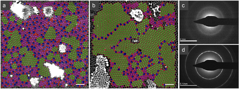
To reveal the uniqueness of the structure of the single-layer amorphous carbon material, this work compares the atomic structure of the single-layer amorphous carbon and the single-layer nanocrystalline carbon samples (Figure 3a and b). The nanograins in the amorphous sample show relatively severe strain with no apparent boundary between grains. Instead, they are separated by an amorphous network with a width of at least three atoms. Thus, the visible image of the traditional crystal domains separated by the grain boundaries no longer applies.
Amorphous diffraction rings confirm the amorphous morphology of single-layer amorphous carbon samples. Nanocrystalline samples have significantly sharper first- and second-order diffraction rings (Figure 3c, d). The atomic model of the amorphous structure should provide new physical images for the universal laws of amorphous materials currently debated in the academic community.

Figure 3. STEM images (a, b) and diffraction images (c, d) of single-layer amorphous carbon and nanocrystalline graphene.
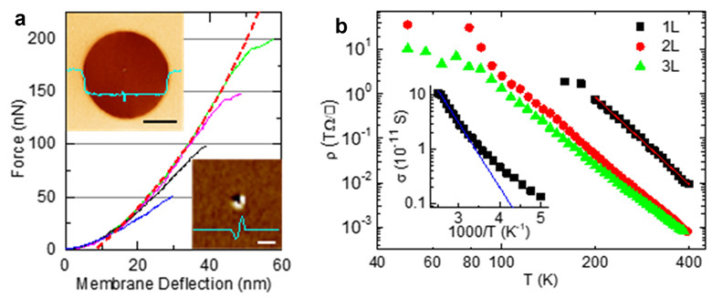
The international team also measured the mechanical and electrical properties of single-layer amorphous carbon samples. They found excellent mechanical stability, even under significant stress (Figure 4a). The samples also showed high levels of electrical performance, similar to that of CVD boron nitride (Figure 4b).

Figure 4. Mechanical (a) and electrical properties (b) of single-layer amorphous carbon material.
The researchers have shown that it is possible to grow a large, stable, and self-supporting single-layer amorphous carbon film. The mechanical and electrical properties could lead to commercial applications in areas such as composite anti-corrosion coatings, flexible electronic circuit devices, and energy storage. There are also future research directions incorporating graphene into 2D amorphous materials.
Associate Professor Lin Junhao’s group worked with excellent teams from around the world. Teams were led by Professor Sokrates T. Pantelides (Department of Electrical Engineering and Computer Science, Vanderbilt University), Professor Barbaros Özyilmaz (Department of Physics, NUS) and Professor Kazu Suneaga (Department of Mechanical Engineering, University of Tokyo). There was also support for the work from Professor Wang Yun-Peng at the School of Physical Science and Electronics at Central South University.
This work has received strong support from the start-up funding for the Shenzhen Peacock Program, and the Pico Center of Southern University of Science and Technology, among other sources at home and abroad.
Article link: https://www.nature.com/articles/s41586-019-1871-2