SUSTech research group makes significant progress in the study of Magnetic Classification Theory
2026-04-23Ambient-pressure Nickelate Superconductors reach new heights
2026-03-13SUSTech Team Reveals Atomic-Scale Mechanism Governing Thermoelectric Transport in Bismuth Telluride
2026-03-06SUSTech team advances the construction of a tunable 2D “Kondo Superlattice”
2026-01-27Researchers make breakthrough in magnetic geometry-induced quantum geometry and nonlinear transport
2025-06-06The unique structure and extraordinary properties of two-dimensional (2D) materials show great potential in the research and development of next-generation optoelectronic devices. Establishing a correlation understanding of the structure and properties of 2D materials at the atomic scale is the key to in-depth exploration of their physical and chemical properties and to facilitate device research and development.
This understanding can also guide material design to achieve material property transformation or performance improvement through structural modulation. As the booming defect engineering research has found, the intentional introduction of special defect structures into 2D materials enables continuous tuning of the carrier concentration, optical band gap, dipole moment, etc. of 2D materials.

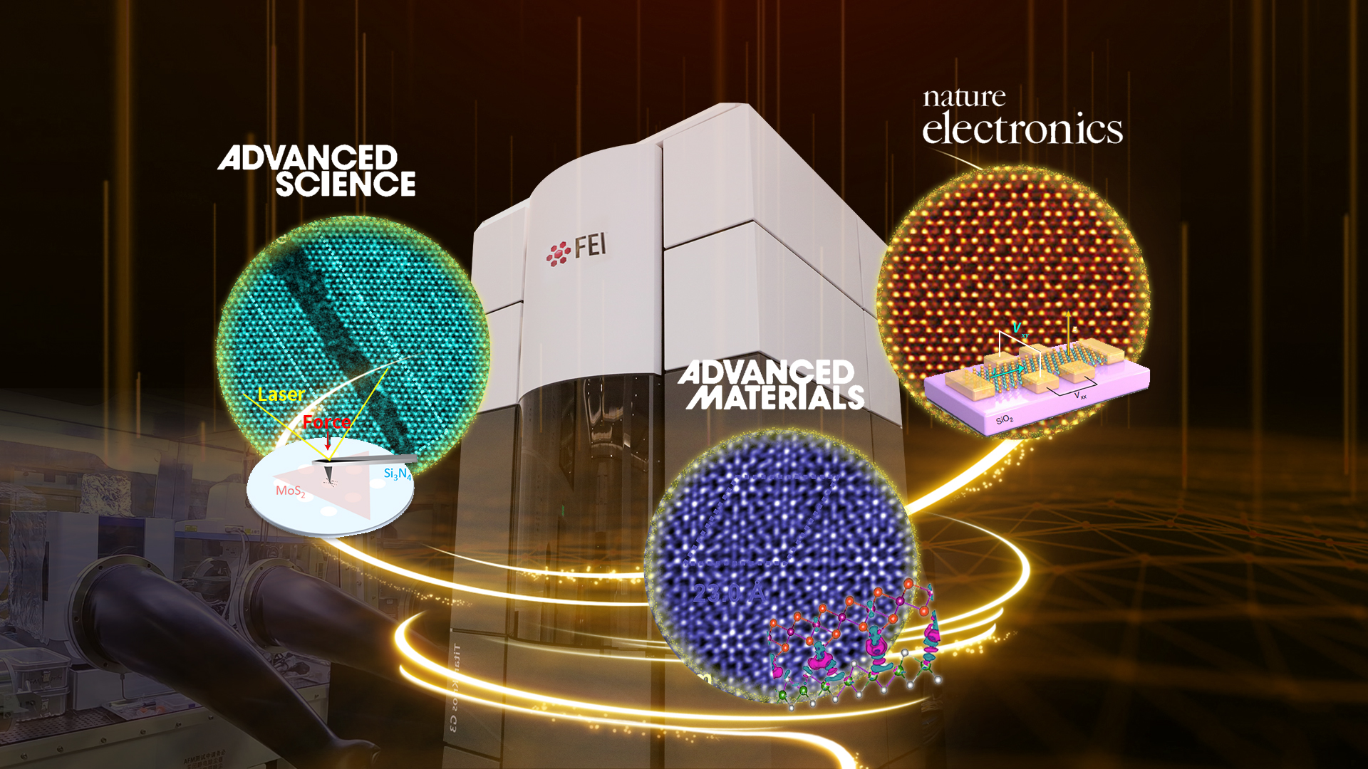
Associate Professor Junhao Lin’s research group of the Department of Physics and the Shenzhen Key Laboratory of Advanced Quantum Functional Materials and Devices at the Southern University of Science and Technology (SUSTech), in collaboration with domestic and overseas research groups, has made a series of research progress in the study of structurally modulated mechanical and magnetic properties in 2D functional materials. Their relevant achievements were published in the journals of Advanced Science, Nature Electronics, and Advanced Materials.
Benefiting from the progress of micro-nano manufacturing technology, ion beam, and electron beam processing can achieve continuous regulation of defect size and concentration within a certain range. However, there are relatively few studies on how the defects introduced in the periodic lattice affect the macroscopic mechanical properties of 2D materials, especially the mechanical failure process under load and stress that mimics a realistic working environment. Therefore, it is of great significance to establish the correlation between defect structures, concentration, and mechanical behavior of 2D materials.
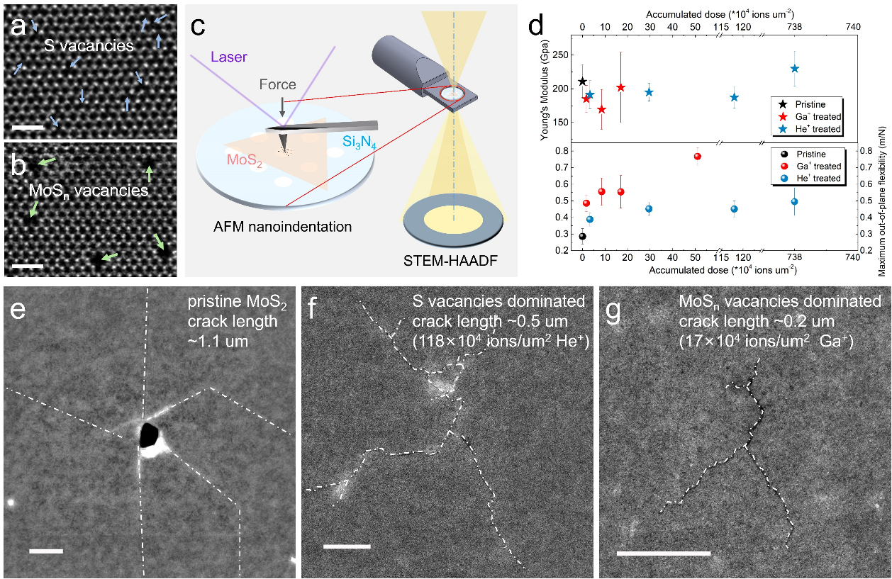
In view of this, Prof. Lin’s research group used helium- and gallium-ion- beam lithography to generate a high density of sulfur (S) and MoSn point defects in suspended monolayer MoS2, respectively. By synergistically combining the AFM nanoindentation technology with scanning transmission electron microscopy (STEM) atomic-structure characterization, the effects of different types and concentrations of point defects on the mechanical properties such as Young’s modulus, fracture strength, and atomic-scale fracture behavior of monolayer MoS2 were revealed.
By analyzing the atomic structure of crack edges induced by different defects, the researchers found that the defect-induced lattice symmetry breakage promotes the crack deflection or bifurcation, which improves the fracture toughness by enhancing the energy release rate in the fracture process. MD simulations and local strain distribution analysis at the crack tip region show that fusion with defects blunts the crack front and is conducive to preventing brittle crack propagation. This research provides an atomic understanding of fracture mechanics of 2D materials and offers an idea for shortening the brittle crack.
The research results were published in the journal Advanced Science, entitled “Engineering the crack structure and fracture behavior in monolayer MoS2 by selective creation of point defects”.
Graduate student Gang Wang is the first author of this paper. Assoc. Prof. Yun-Peng Wang at Central South University is the co-first author, while Assoc. Prof. Junhao Lin at SUSTech is the only corresponding author. SUSTech is the first affiliation of this paper.

Figure 1. Mechanical properties of pristine/defective monolayer MoS2 and STEM characterization of the fracture traces after indentation test
The structure of 2D materials can not only be modulated by post-processing, but also by regulating the growth parameters to achieve modulation or new structural assembly during synthesis. Prof. Lin’s group at SUSTech, in collaboration with Prof. Zheng Liu at Nanyang Technological University (NTU), Prof. Jiadong Zhou at Beijing Institute of Technology (BIT), and Prof. Xingji Li at Harbin Institute of Technology (HIT), used the chemical vapor deposition (CVD) method to realize the synthesis of ultrathin 2D magnetic materials Cr5Te8 with selective trigonal and monoclinic phases by regulating the growth temperature and cooling rate.
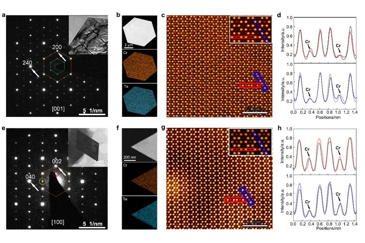
Selected-area electron diffraction (SAED) and atomic-resolution high-angle annular dark-field (HAADF)-STEM imaging have precisely determined the phase structure changes caused by the different intercalation positions of Cr atoms, thus confirming the tunability of the phase structure of the Cr5Te8 self-intercalation system. Combined with magnetic tests and theoretical calculations, the researchers revealed the significant effect of the phase structure on the magnetic order. By regulating the phase structure and thickness, the Curie temperature (TC), the temperature above which certain materials lose their permanent magnetic properties, can be obtained as high as 200K. In addition, they also found that the more disordered monoclinic phase Cr5Te8 has a huge anomalous Hall effect (σAHE ~ 650 Ω-1cm-1, θAHE ~ 5%). This work provides a route to the controllable and scalable synthesis of 2D magnetic materials, and reveals the great promise of Cr5Te8 nanosheets in magnetoelectronic and spintronic applications.
The research results were published in the journal Nature Electronics, entitled “Phase engineering of Cr5Te8 with colossal anomalous Hall effect”.
Dr. Bijun Tang at NTU is the first author of this paper. Dr. Xiaowei Wang at NTU, Dr. Mengjiao Han at SUSTech, and Dr. Xiaodong Xu at HIT are the co-first authors, while Prof. Zheng Liu at NTU, Prof. Xingji Li at HIT, Prof. Jiadong Zhou at BIT, and Assoc. Prof. Junhao Lin at SUSTech are the corresponding authors.

Figure 2. Atomic morphology of trigonal and monoclinic Cr5Te8 crystals
Another route to modulate the structure of 2D materials is epitaxial growth with the confinement of the substrate lattice. However, conventional covalent heteroepitaxy has stringent requirements on the lattice matching and processing compatibility requirements. Prof. Lin’s group, in collaboration with Prof. Hao Zeng at the University at Buffalo, the State University of New York (UB), and Prof. Hou Yanglong at Peking University (PKU), proposed an epitaxial growth mechanism driven by interfacial dative bond formation.
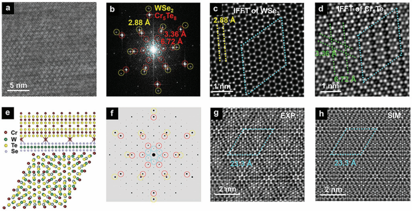
Based on this mechanism, covalent magnetic single-crystal Cr5Te8 was epitaxially grown on monolayer WSe2 and obtained a fully commensurate matching 3×3 (Cr5Te8)/ 7×7 (WSe2) Moiré supercell. 2D Cr5Te8 crystals grown by dative epitaxy exhibit square magnetic hysteresis, suggesting minimized interfacial defects that can serve as pinning sites. The “dative epitaxy” approach proposed by the collaborative research team, as a conceptually distinct paradigm of thin-film epitaxy, takes full advantage of covalent epitaxy with chemical bonding for fixing the atomic registry and crystal orientation, while circumventing its stringent lattice matching and processing compatibility requirements. Conversely, it ensures the full flexibility of vdW epitaxy, while avoiding its poor orientation control.
The research results were published in the journal Advanced Materials, entitled “Dative Epitaxy of Commensurate Monocrystalline Covalent van der Waals Moiré Supercrystal”.
Dr. Mengying Bian at PKU and Dr. Liang Zhu at SUSTech are the co-first authors of this paper, while Prof. Hao Zeng at UB, Prof. Yanglong Hou at PKU, and Assoc. Prof. Junhao Lin at SUSTech are the corresponding authors.

Figure 3. HAADF-STEM analysis of the Cr5Te8/WSe2 moiré superlattice
Paper links (In order of appearance above):
Advanced Science:
Nature Electronics:
Advanced Materials: