
Ambient-pressure Nickelate Superconductors reach new heights
2026-03-13SUSTech Team Reveals Atomic-Scale Mechanism Governing Thermoelectric Transport in Bismuth Telluride
2026-03-06SUSTech team advances the construction of a tunable 2D “Kondo Superlattice”
2026-01-27Researchers make breakthrough in magnetic geometry-induced quantum geometry and nonlinear transport
2025-06-06SUSTech hosts IOP Forum with President of Institute of Physics Sir Keith Burnett
2025-03-26Thermoelectric material is a kind of new energy material that can realize the direct mutual conversion of thermal energy and electrical energy through the directional movement of internal carriers with the temperature difference. Thermoelectric devices prepared from thermoelectric materials have the characteristics of small size, high reliability, wide operating temperature range, and no noise. They have great potential for development in both military and civilian applications.
The performance (ZT) of thermoelectric materials is jointly determined by the material’s intrinsic electrical conductivity (σ), Seebeck coefficient (S), and thermal conductivity (κ), but these parameters are strongly coupled together, making harvesting high ZT values a great challenge.
Chair Professor Jiaqing He’s team from the Department of Physics at the Southern University of Science and Technology (SUSTech) has recently made a series of important progress in the research of GeTe-based thermoelectric materials.
The related results were published online in Science Advances, Nature Communications, and Energy & Environmental Science. Their studies take the two-dimensional defect structure in GeTe-based thermoelectric material as the research objects to explore their formation mechanism, working mechanism, and a way to artificially modulate the defect. These works are expected to promote the application process of thermoelectric materials in medium- and high-temperature regions.
In recent years, through a comprehensive and detailed analysis of the microstructure and transport properties of thermoelectric materials, researchers have mastered several effective partial decoupling methods to optimize the performance of thermoelectric materials. Scattering phonons by scale defects is considered a classic strategy to suppress lattice thermal conductivity. Previous studies by Prof. He’s research team also showed that the introduction of layer-like defects in GeTe-based samples could effectively scatter mid- and low-frequency phonons and improve the sample’s performance (Average ZT value).
Theoretically, the ability of defects to scatter phonons is closely related to parameters such as the density and size of defects. Although the introduction of defects of various scales has been studied, the artificial regulation of related defect parameters and related mechanisms are rarely reported. The directional preparation of internal defect density and defect size is undoubtedly very beneficial to promote the research of thermoelectric materials. In particular, for the two-dimensional defect structure in GeTe-based samples, its formation mechanism and action mechanism are still to be explored.
Their first paper, entitled “Strain-induced van der Waals gaps in GeTe revealed by in-situ nano-beam diffraction,” was published in Science Advances.
In GeTe-based thermoelectric materials, an atomic-scale van der Waals defect has been reported many times. The experimental data show that its existence can effectively reduce the lattice’s thermal conductivity and improve the thermoelectric conversion efficiency. However, its generation mechanism has been controversial, which also hinders more in-depth research.
In theory, the formation and movement of defects are closely related to the field environment, such as the stress field. However, traditional methods make it extremely difficult to directly characterize the stress-strain field at the micro-nano scale. Due to its high resolution, TEM has unique advantages in micro- and nano-scale observation. Several advanced microscopic methods, such as geometric phase analysis, nano-beam diffraction technology, electron holography technology, etc., make the sample’s strain field characterization possible.
In order to reveal the strain changes before and after defect formation, the most direct way is to perform in-situ observations. Based on this, in situ nano-beam diffraction was used to monitor the strain before and after the formation of van der Waals defects (two-dimensional surface defects) in a fixed region (as shown in Figure 1). By choosing the same reference diffraction spot, the strain changes before and after van der Waals defect formation can be directly compared. The experimental results show that the strains in the corresponding regions of the annealed samples are relaxed.
The researchers reasoned that there must be some connection between the relaxation of strain and the growth of van der Waals defects. As shown in Figure 2, Prof. He’s team directly observed that the growth process of van der Waals defects is slowly growing from one end to the other. Through theoretical calculations and related kinetic analysis, we concluded that this growth mechanism is similar to the climbing of dislocations. That is, a large number of discrete cation vacancies (zero-dimensional) in the sample can aggregate and reconstruct into two-dimensional defects under the action of strain. This paper resolves the long-standing controversy over the origin of van der Waals defects in the GeTe system, paving the way for introducing van der Waals defects into other systems.
Yong Yu, a joint doctoral student of SUSTech and the National University of Singapore (NUS) and member of Prof. Jiaqing He’s team, is the first author of this paper. Professor Jiaqing He is the corresponding author, and SUSTech is the first affiliation.
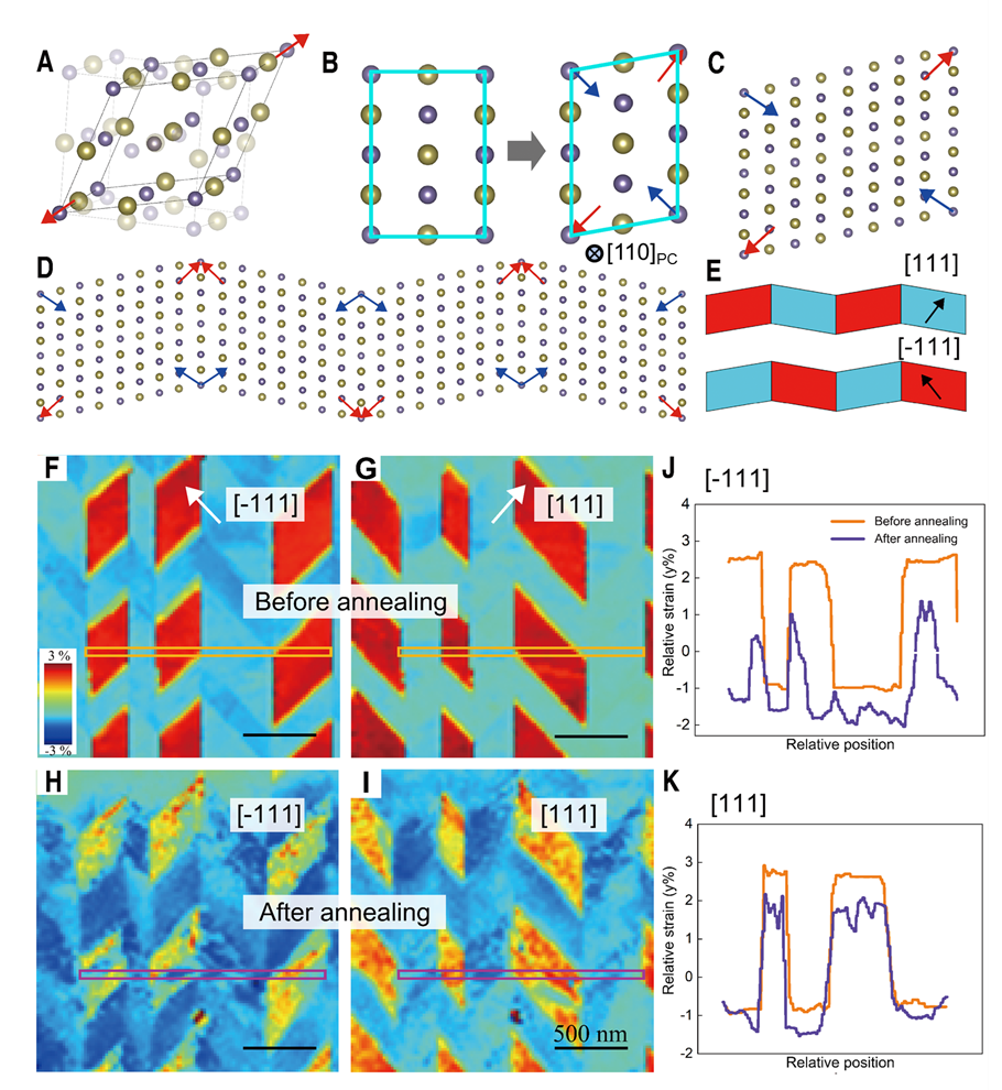
Figure 1. Changes in strain field before and after van der Waals 2D defect generation.
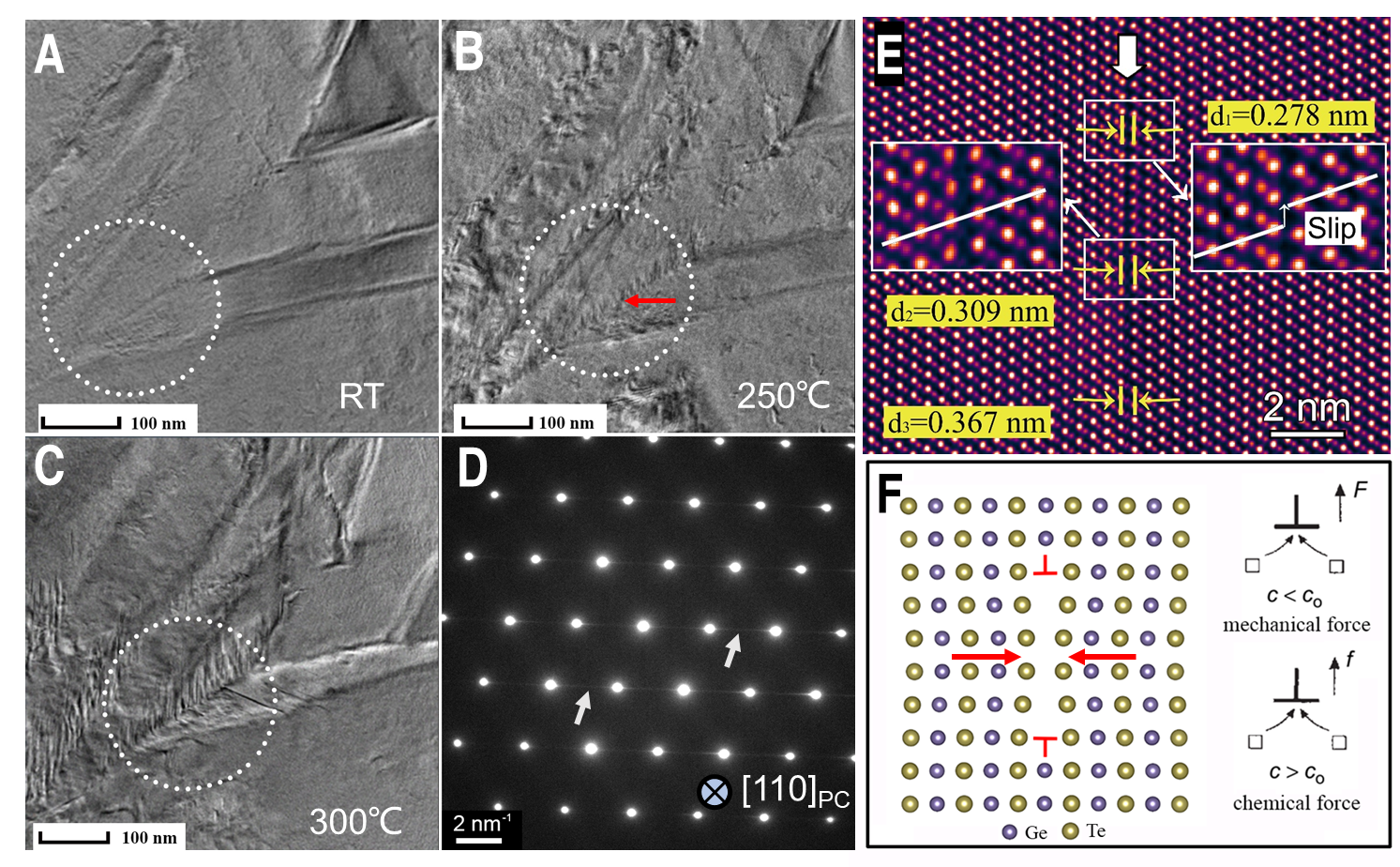
Figure 2. In situ observation of van der Waals 2D defect growth and analysis of its origin using dislocation theory.
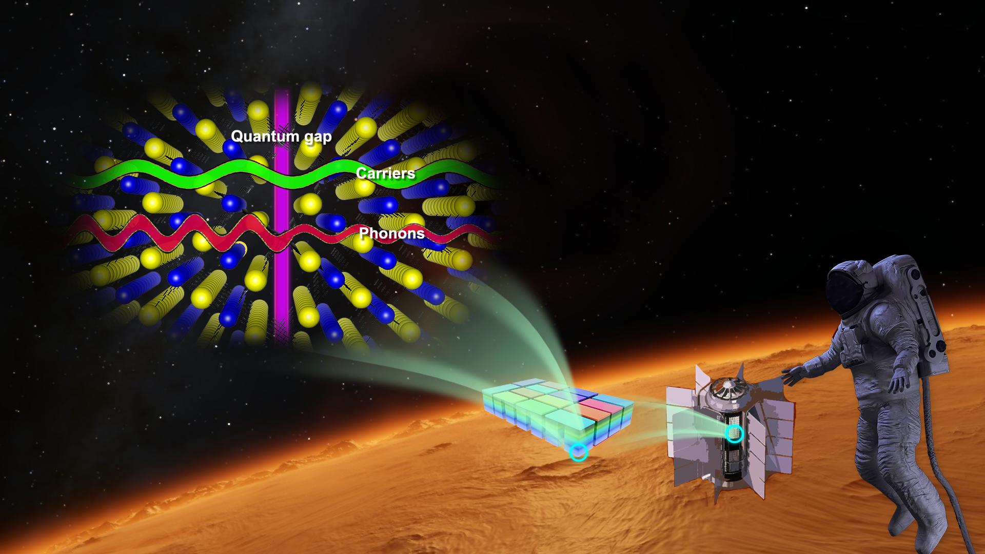
The group’s second paper, entitled “Tunable quantum gaps to decouple carrier and phonon transport leading to high-performance thermoelectrics,” was published in Nature Communications.
Traditionally, the main role of defect engineering is considered to scatter phonons to reduce lattice thermal conductance. It is generally believed that defects of relevant scales scatter both phonons and carriers (reduce mobility). However, many reports show that reasonable introduction of defects can always improve the ZT value for the layer-like defect structure. This means that the presence of this type of defect does not necessarily reduce the mobility significantly, and this interesting experimental result prompts us to rethink the role of this type of defect structure.
In this paper, taking the van der Waals defect in the GeTe system as an example, the Coulomb potential of the defect at room temperature and high temperature is obtained by electron holography (Figures 3 & 4). The transmission coefficient of this potential well is calculated according to the scattering equation, and its value is very close to 1, which means that this defect hardly scatters carriers. Furthermore, the phonon spectrum and phonon scattering rate of GeTe with defects are calculated in this paper.
The results show that the van der Waals defects can significantly improve the scattering rate, which is consistent with the breaking of the translational symmetry of GeTe observed by microstructural analysis and the experimental results. The measured reduced thermal conductivity fits well. This work also found that adding a trace amount of rare earth element Re can effectively broaden the spacing distribution of two-dimensional quantum defects, enabling such defects to effectively scatter wider-band phonons, thereby further reducing the lattice thermal conductance.
In general, the inclusion of this special defect structure can achieve the effect of synergistically optimizing the electrical and thermal transport properties, and achieve the purpose of carriers and phonons decoupling. Finally, this work comprehensively regulated the distribution of defects in the sample and optimized its carrier concentration, so that the lead-free GeTe system obtained the highest ZT value of 2.6 and an average ZT value of 1.6, which are the record values reported so far.
Yong Yu is the first author of this paper. Xiao Xu, a postdoctoral fellow of the Department of Physics at SUSTech, and Yan Wang, a doctoral student at SUSTech, are the co-first authors. Research Assoc. Prof. Lin Xie and Prof. Jiaqing He are the corresponding authors, and SUSTech is the first affiliation.
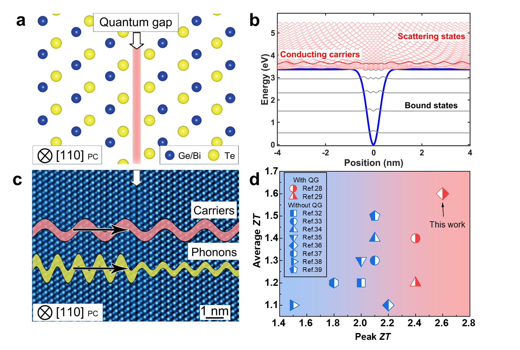
Figure 3. Two-dimensional quantum defects and their role in Ge-Bi-Te alloys. (a) Structural model of a 2D quantum defect. (b) The potential well at the quantum defect and the resulting quantum state. (c) Schematic illustration of the decoupling of carriers and phonons transport by 2D quantum defects. (d) Statistical plot of the reported performance in the lead-free GeTe system, where blue is the system without 2D quantum defects, and red data points are systems with 2D quantum defects.
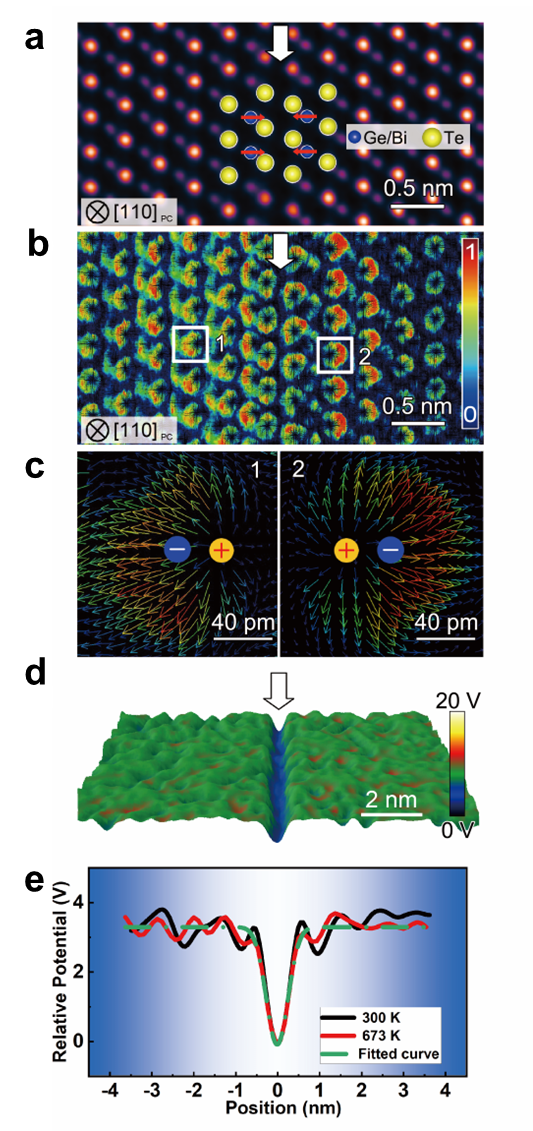
Figure 4. Structure of a 2D quantum defect. (a) Atomic image of a 2D quantum defect. (b & c) Atomic-scale electric field distribution of a 2D quantum defect. (d) 3D schematic diagram of the Coulomb potential distribution at the 2D quantum defect. (e) Coulomb potential distributions at room temperature and high-temperature 2D quantum defects.
Prof. He’s group also claimed that the micro-structural density of gap-like structures (named GLSs in this article) of Sb2Te3(GeTe)n could be manipulated precisely by tuning the compounds ratio of GeTe to Sb2Te3. This last study, entitled “Highly Tailored Gap-like Structure for Excellent Thermoelectric Performance,” has been published in Energy & Environmental Science, one of the most famous international scientific journals.
In this work, they conducted a further optimization of the size of the GLSs via appropriate Re doping. According to the experimental data, the band structure and hole density were modulated simultaneously in Re-doped Sb2Te3(GeTe)17 samples, leading to a higher transport property. Eventually, a competitive high ZT peak value and ZT average value were achieved after highly tailoring the GLSs. In addition, a single-stage thermoelectric module based on the p-type Sb2Te3(Ge0.995Yb0.005Te)17 materials can provide an exceptional output power density, enlightening the huge application potential of highly tailored methods about GLSs for obtaining extremely high TE performance.
In summary, this study enhanced the power factor and reduced the thermal conductivity of GeTe-based TE samples simultaneously, leading to a significant improvement in the performance over the whole temperature range. Thus, a maximal figure of merit ZTmax ~ 2.4 at 773 K and a high ZTave value of 1.5 from 323 to 773 K were realized. From the perspective of the TE module, a record high power density value of 1.25 W cm-2 and a remarkable output power of 2.65 W over the hot-side temperature of 773 K were obtained. The highly tailoring methods of GLSs in this work and their noteworthy effect on thermoelectric transports can reinforce the investigation mechanism and shed light on the development of other TE-based materials.
Xiao Xu is the first author of this paper. Xixi Liu, Research Asst. of Prof. Jiaqing He’s team, and Dr. Yi Huang of SUSTech are the co-authors. Prof. Jiaqing He is the only corresponding author, and SUSTech is the first affiliation.
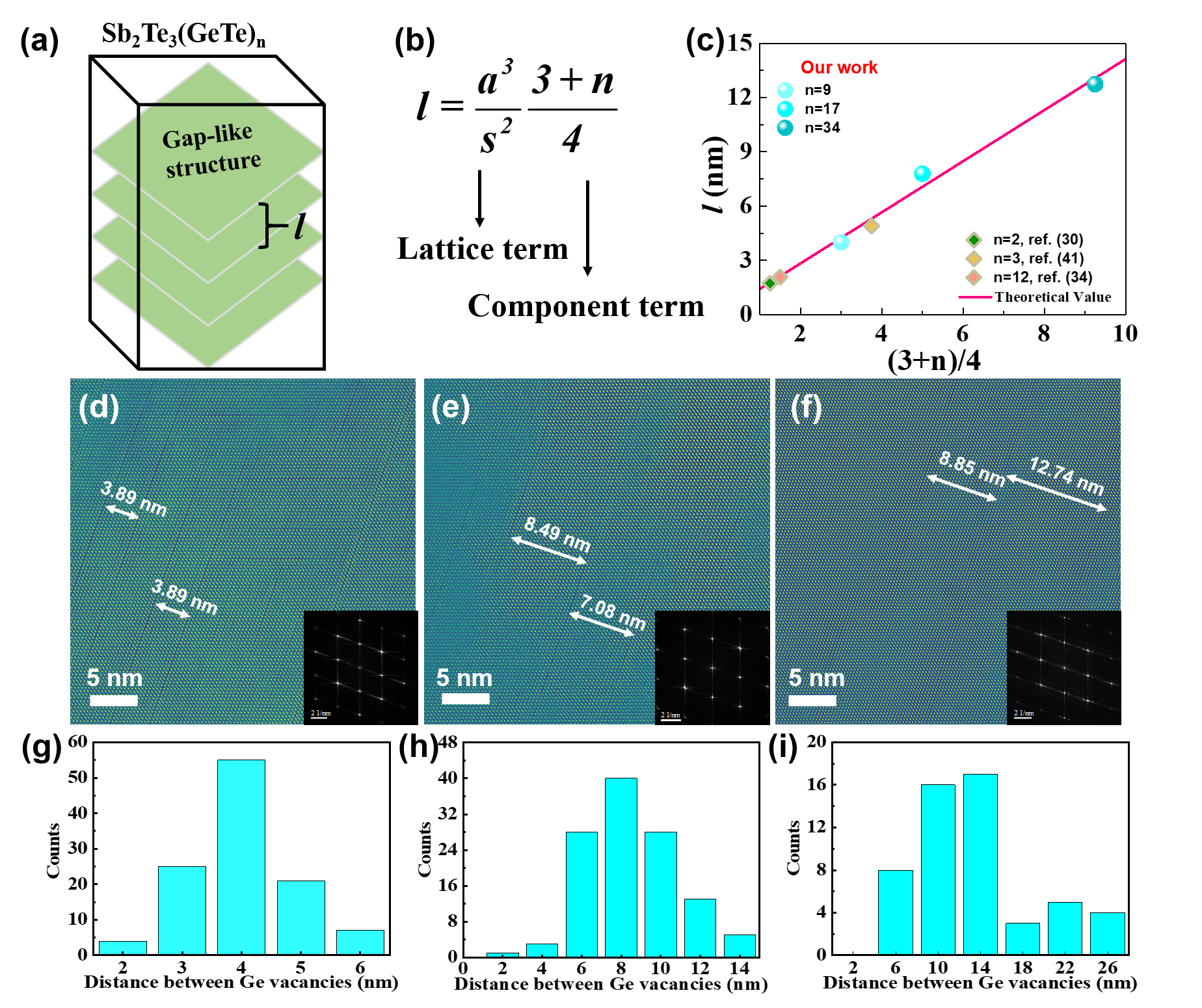
Figure. 5 (a) Schematic diagram of layer-like structure in Sb2Te3(GeTe)n, (b) derived equation of characteristic length l, (c) experimental and theoretical values between components and l in this work and literature, (d–f) HAADF-STEM images of Sb2Te3(GeTe)9, Sb2Te3(GeTe)17 and Sb2Te3(GeTe)34, and (g-i) histograms of the distribution of distances between layer-like structures in the corresponding samples.
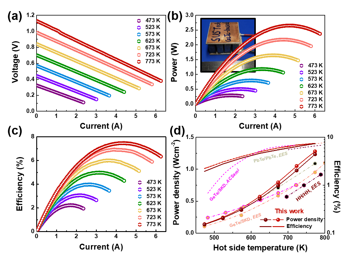
Figure. 6 (a) output voltage, (b) output power, and (c) efficiency of Sb2Te3(Ge0.995Yb0.005Te)17/Pb1-xSbxTe thermoelectric module with measured current at different hot-end temperatures. (d) measured in this work. Comparison of efficiency and power density with literature reports with similar module size and footprint.
The above works were financially supported by the China Postdoctoral Science Foundation Funded Project, National Natural Science Foundation of China (NSFC), and Science, Technology, and Innovation Commission of Shenzhen Municipality. The authors also acknowledge the support of the Core Research Facilities and Center for Computational Science and Engineering at SUSTech for its TEM resources and calculation resources, respectively.
Papers links (In order of appearance above):
Science Advances:
Nature Communications:
Energy & Environmental Science:
[-]08162804_46525.jpg)
WeChat public account
Copyright C 2022 SUSTech.All rights reserved. | Designed by Unison.
WeChat public account
Copyright C 2022 SUSTech.All rights reserved. | Designed by Unison.