
SUSTech research group makes significant progress in the study of Magnetic Classification Theory
2026-04-23Ambient-pressure Nickelate Superconductors reach new heights
2026-03-13SUSTech Team Reveals Atomic-Scale Mechanism Governing Thermoelectric Transport in Bismuth Telluride
2026-03-06SUSTech team advances the construction of a tunable 2D “Kondo Superlattice”
2026-01-27Researchers make breakthrough in magnetic geometry-induced quantum geometry and nonlinear transport
2025-06-06The century-long development of surface sciences has witnessed the discoveries of a variety of quantum states. In a recently published article, researchers observe spectroscopic signature of the novel “obstructed surface states” on the (0001) plane of SrIn2P2, a candidate “obstructed atomic insulator (OAI)”. Due to structural reconstruction, the surface state undergoes an adiabatic evolution and split into two branches, the upper of which being spatially localized with unusual negative differential conductance.
Associate Professor Chang Liu’s research group from the Department of Physics and Shenzhen Institute for Quantum Sciences and Engineering (SIQSE) at the Southern University of Science and Technology (SUSTech), in cooperation with the research groups of Associate Professors Yue Zhao and Qihang Liu, also of the Department of Physics at SUSTech, has recently made progress in the study of the electronic structure of OAIs.
Their paper, entitled “Spectroscopic Signature of obstructed surface states in SrIn2P2”, was published in the journal Nature Communications.
At the surface of solid materials, the wave function of electrons is confined at the interface between the sample and the vacuum, and induces distinct dispersion compared with the bulk one. These states are called the “surface electronic states”. Typically, the properties of the surface states are determined by various physical and chemical environments at the surface atomic sites. In other words, the atoms at the surface define the surface.
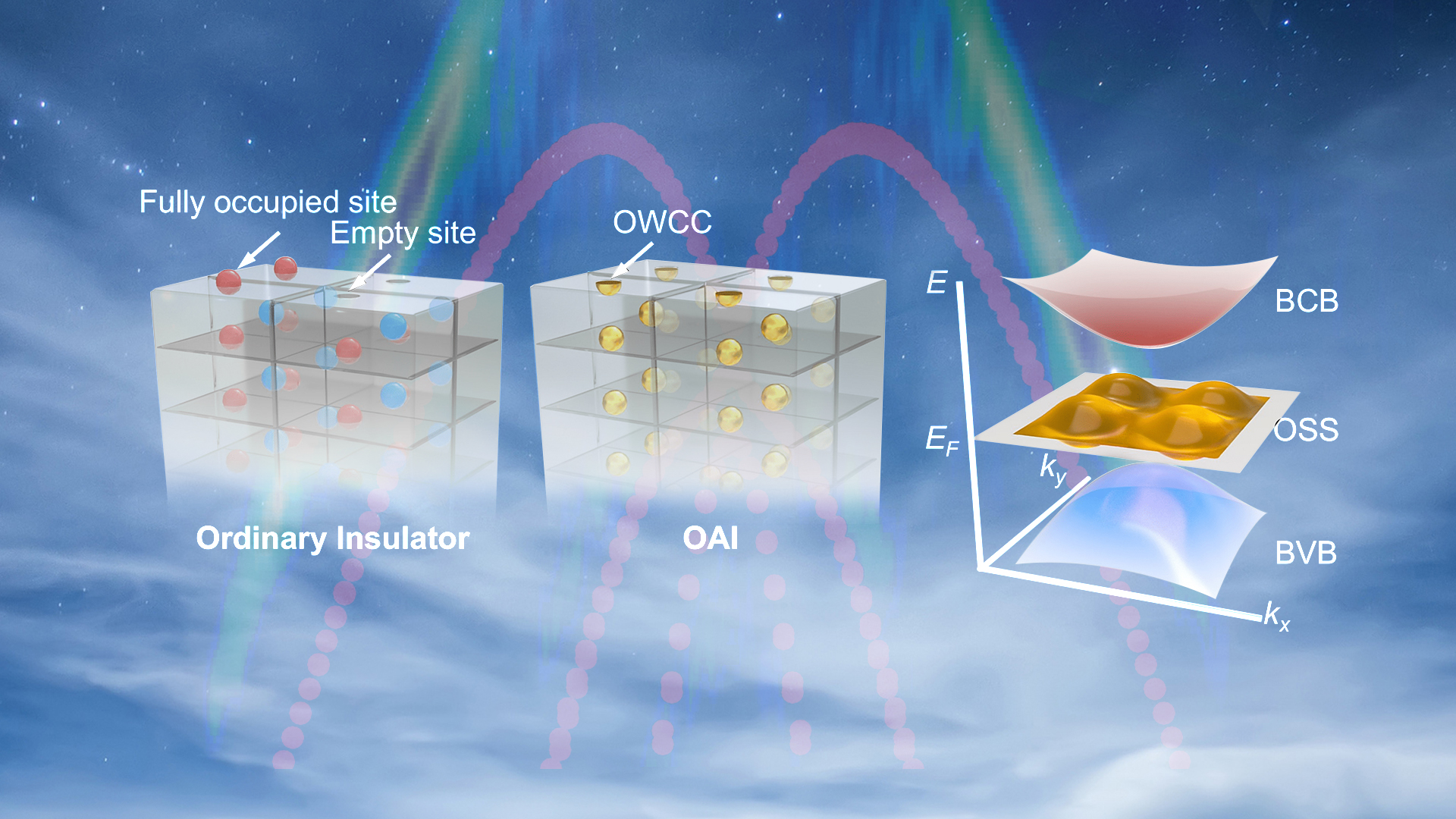
It is widely accepted that when a surface termination is formed in an ordinary insulator, the atoms on the topmost layer are either completely peeled off or left intact at the termination (Fig. 1a). Recently, however, a new class of insulators has been predicted theoretically, whose ground-state charge centers are located in some “vacant sites” where no atoms exist (such as the middle position between two van der Waals atomic layers). If the natural cleavage plane of the sample happens to pass through these sites, there will be “half electrons” for each vacant site (a.k.a. “filling anomaly”, Fig. 1b). Thus, at the interface or domain walls of the sample, there exists an “obstructed surface state (OSS)” with half the electron occupation, much like the three-dimensional version of the Su-Schrieffer-Heeger model.
Due to its half-filled nature, this novel surface state necessarily crosses the Fermi level, making the interface conductive (Fig. 1c). Insulators with OSSs are called OAIs. It is theorized to exist in various materials, such as electronic compounds, high-order topological insulators, and hydrogen evolution reaction electrocatalysts, etc. In principle, these half-filled vacant sites are active for ligand adsorption and electron transfer, making OAIs ideal platforms for surface catalysis and related applications. In a sense, it can be considered that the appearance of OAIs generalizes the definition of “surface”; that is, the electronic states of the surface define the surface.
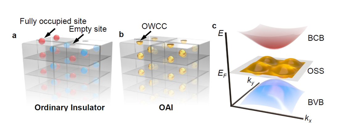
Figure 1. Schematic diagram for ordinary insulator, OAI, and OSS
According to first-principles calculations, SrIn2P2 is a candidate OAI. Its natural cleavage plane is the (0001) plane, which cuts through the aforementioned “vacant sites” [a.k.a. “obstructed Wannier charge centers (OWCCs)”]. Thus, if the surface of the sample does not undergo reconstruction, the researchers should be able to observe metallic OSSs. In this paper, they studied the electronic structure of SrIn2P2 using scanning tunneling microscopy (STM), angle-resolved photoelectron spectroscopy (ARPES), and first-principles calculations, and found that things are not that simple.
The STM topography study on the (0001) cleavage plane of SrIn2P2 found a stripe-like surface topography and √3 x 1 surface reconstruction, indicating that the surface of SrIn2P2 is not an ideal OAI surface (Fig. 2a). The results of scanning tunneling spectroscopy further show that on the entire sample surface, there is a strong differential conductance peak with a width of only 0.4 eV at about 1 eV above the Fermi surface and a negative differential conductance region above the conductance peak (Fig. 2a). This suggests that although metallic surface states do not exist, there is a real-space localized surface electronic state, most likely associated with the OWCCs.
For electronic states below the Fermi level, ARPES studies have discovered surface state energy bands with linear dispersion (Fig. 2b). Therefore, the researchers did not find a conductive electronic state through the Fermi surface on the surface of SrIn2P2 but observed two energetically separated surface states. Combined with first-principles calculations, they found that the theoretically predicted OSSs would adiabatically evolve into the experimentally observed two branches of surface states that are located above and below the Fermi level during the surface reconstruction process (Fig. 2c). Importantly, the correspondence between surface states and the OWCCs remains unchanged during the evolution, which explains the real-space localized nature of the surface state branch above the Fermi level.
Figure 2. Electronic structure of SrIn2P2 was studied comprehensively by STM, ARPES, and DFT. (a) STM topography and characteristic scanning tunneling spectra, showing √3 x 1 surface reconstruction, strong differential conductance peak above the Fermi level, and negative differential conductance above the conductance peak. (b) ARPES band diagram, showing surface states (SS) with linear dispersion. (c) DFT calculated surface electron density (upper panel) and the band structure (lower panel). The differential conductance peak observed by STM corresponds to the upper branch of surface states, and the linearly dispersed electronic states observed by ARPES correspond to the lower branch of surface states.
This work reveals the electronic structure of obstructed atomic insulators for the first time, and discovers the OSS-derived localized surface electronic states in real space, which has guiding significance for further research on obstructed atomic insulators and the development of new surface catalysts.
Graduate students Xiang-Rui Liu and Yuntian Liu and postdoctoral researcher Hanbin Deng are the co-first authors of this paper. Associate Professors Yue Zhao, Qihang Liu, and Chang Liu are the corresponding authors, and SUSTech is the first affiliation of the paper.
This research was supported by the National Natural Science Foundation of China (NSFC), Key-Area Research and Development Program of Guangdong Province, and the Highlight Project of the College of Science at SUSTech.
Paper link:
[-]08162804_46525.jpg)
WeChat public account
Copyright C 2022 SUSTech.All rights reserved. | Designed by Unison.
WeChat public account
Copyright C 2022 SUSTech.All rights reserved. | Designed by Unison.