
SUSTech research group makes significant progress in the study of Magnetic Classification Theory
2026-04-23Ambient-pressure Nickelate Superconductors reach new heights
2026-03-13SUSTech Team Reveals Atomic-Scale Mechanism Governing Thermoelectric Transport in Bismuth Telluride
2026-03-06SUSTech team advances the construction of a tunable 2D “Kondo Superlattice”
2026-01-27Researchers make breakthrough in magnetic geometry-induced quantum geometry and nonlinear transport
2025-06-06Two-dimensional van der Waals (vdW) heterostructures are considered to be the best route for exploring two-dimensional (2D) physics and device applications. Among the combinations of stacking components, particular attention is focused on van der Waals superconductor heterostructures (vdWSHs), which are made by stacking 2D superconductors with other materials. High-quality preparation of 2D vdWSHs provides a platform for creating superconducting proximity effects, Josephson junctions, superconducting diodes, and Majorana-based quantum computation.
To fabricate vdWSHs from specific materials and with a particular stacking order, mechanical assembly has been widely used in experiments. However, such mechanically assembled stacking can result in imperfect vdW interfaces, difficulty in stacking, and low yields for effective vdWSHs. The vdW epitaxy method has been used successfully to grow vdWSHs, but none of these approaches has achieved the large-scale fabrication of vdWSHs, owing to the environmental sensitivity and lack of structural stability of the 2D superconductors. Therefore, a general strategy for growing wafer-scale vdWSHs, combining 2D superconductors with controllable thickness, is urgently needed.
Associate Professor Junhao Lin’s research group from the Department of Physics and Shenzhen Key Laboratory of Advanced Quantum Functional Materials and Devices at the Southern University of Science and Technology (SUSTech) and Professor Libo Gao’s research group from the School of Physics at Nanjing University have recently made a breakthrough in the study of the stack growth mechanism of wafer-scale vdWSHs.
Their findings, entitled “Stack growth of wafer-scale van der Waals superconductor heterostructures”, were published in the top international journal Nature.
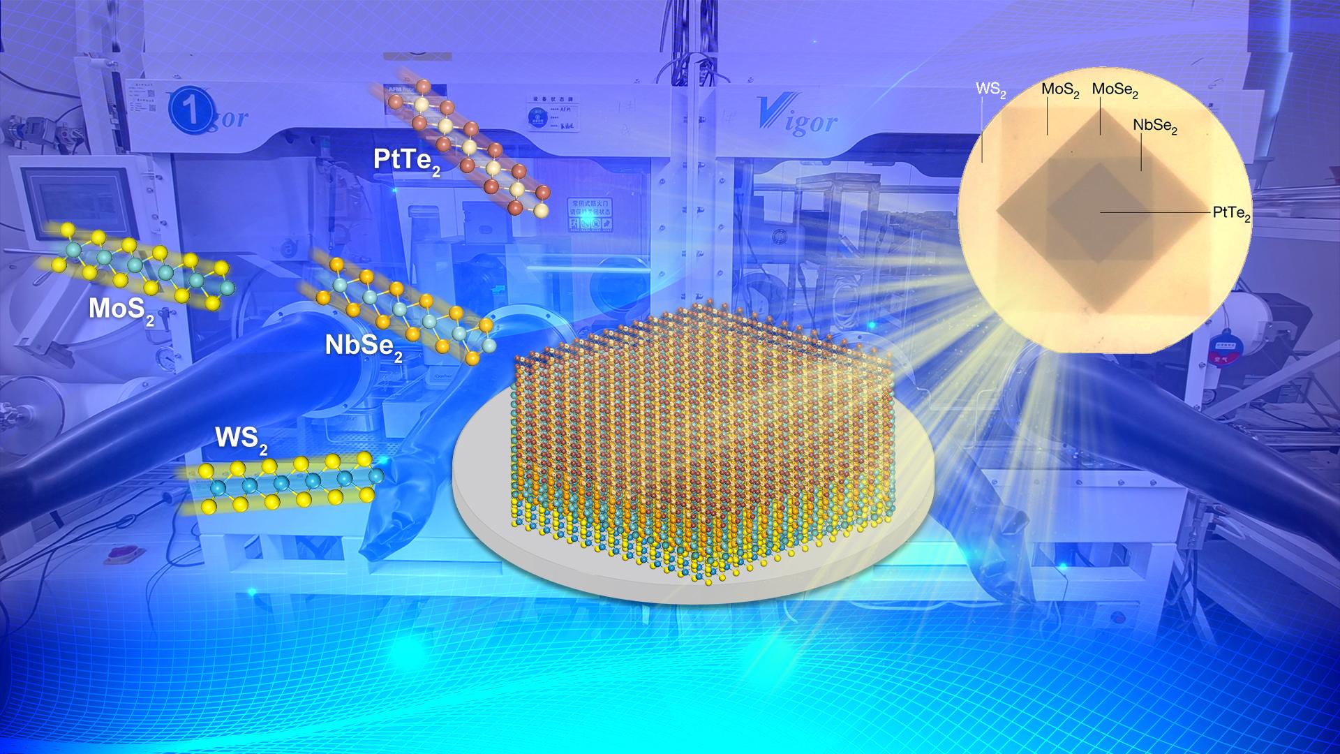
Despite thousands of 2D materials being created using various stacking combinations, hardly any large 2D superconductors can be stacked intact into vdW heterostructures because of their unstable structure, e.g., NbSe2, greatly restricting the applications for such devices. To overcome this problem, the researchers developed a new ‘high-to-low’ temperature strategy for controllably growing stacks of multiple-layered vdWSH films at a wafer scale (Figure 1), in which ‘high’ and ‘low’ refer to the various growth temperatures needed for different 2D materials. The number of layers of 2D superconductors in the vdWSHs can be precisely controlled, and the corresponding atomic-scale structural analyses reveal the high quality of stacking structures using a double spherical aberration scanning transmission electron microscope (STEM).
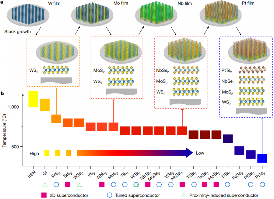
Figure 1. Stack growth of multiblock vdWSHs guided by the high-to-low strategy
In this work, the researchers reported that a high-to-low strategy has unique advantages in controllably growing wafer-scale, multiblock vdWSH films. On the one hand, the method is a multicycle two-step vapour-deposition process; in other words, the growth temperature of each layer of two-dimensional material is lower than that of its precursor material, which can avoid the decomposition, etching, or alloying in the pregrown bottom 2D materials and therefore achieve the specific wafer-scale vdWSH thin film (as shown in Figure 2); on the other hand, the stack-growth strategy allows better retention of the high crystal quality, high environmental stability, and high thermal stability of the 2D crystal films, making it possible to prepare vdWSH films with clean interfaces and intact superconducting properties. Through further regulating the temperature, the number of layers of 2D superconductors in the vdWSHs can be precisely controlled, and the precise nature of the vdWSH films can be programmed in the stacking arrangements, acting somewhat like the building blocks of atomic-scale Lego.
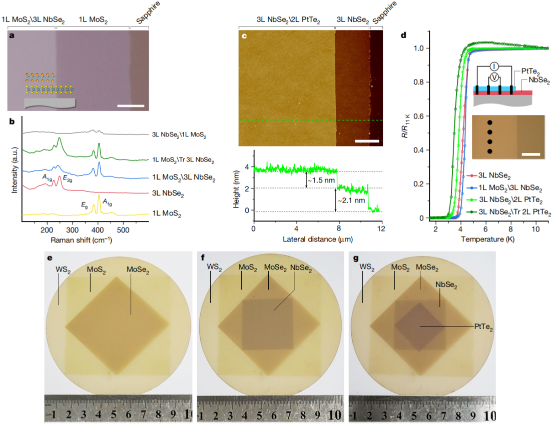
Figure 2. Generality of the high-to-low strategy and homogeneity of the wafer-scale vdWSH films
Two-dimensional superconductors have high surface activity, which is easily oxidized by air and adsorb hydrocarbons in the environment, which seriously restricts the characterization of samples and physical property tests. The glove box interconnection system (GIS) with full inert atmosphere protection built by Prof. Lin’s group (Figure 3) realized full inert atmosphere protection from sample growth, transfer, post-processing, atomic structure characterization, and physical property testing, which greatly reduced the surface oxidation and pollution of HEA NPs. It has the unique advantage of studying the intrinsic structure and growth mechanism of 2D vdWSH films with high surface activity.
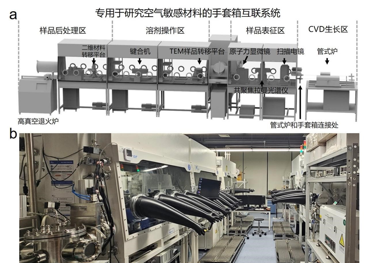
Figure 3. Schematic diagram of glove box interconnection system (top) and the related photograph (bottom)
The team combined the high-to-low strategy growth of multi-block vdWSH films with the GIS to achieve the layer-by-layer elemental distribution and atomic structure characterization of intrinsic samples from different perspectives using high-angle annular dark-field STEM. As shown in Figure 4, the researchers have demonstrated the heterostructure films with various layers and stacking arrangements, and proved the controllability of the number of layers of NbSe2 by the energy-dispersive X-ray spectroscopy (EDS) mappings. Using this growth strategy, they have successfully grown more than 26 double-block, 15 triple-block, 5 four-block, and 3 five-block vdWSH films.
The corresponding HAADF-STEM imaging shows that the typical honeycomb lattice of 1L NbSe2 grown on a 1L WS2 film has a lower density of atomic defects than that of the monolayer grown on a substrate, indicating high crystal quality. Furthermore, they will form various moiré superlattices for lattice-mismatched TMDCs with different metal components, and the twist angle was verified by the fast Fourier transform (FFT) patterns. The twist angle is also altered with the change of lattice mismatch degree. The statistical results display that the crystal domain splicing of angle dependence does not affect the superconducting properties in vdWSH films. These results further proved that the high-to-low strategy can stack grow high-quality vdWSH films at wafer scale with an excellent universality.

Figure 4. Crystalline structure of multiblock vdWSH films
This work has developed a general high-to-low strategy to stack and grow various multiblock vdWSHs at a wafer scale. Highly crystalline 2D superconductors can be successfully stacked in these vdWSHs, and their thickness can be precisely controlled. Atomic structural characterization combined with GIS revealed the key role of high-to-low strategy in the grown mechanism and crystalline quality of vdWSH films.
Zhenjia Zhou, a Ph.D. student from Nanjing University, and Fuchen Hou, Research Assistant Professor from the Department of Physics at SUSTech, are the co-first authors of this paper. Profs. Libo Gao and Jie Xu from Nanjing University and Assoc. Prof. Junhao Lin from SUSTech are the co-corresponding authors.
This work was supported by the National Natural Science Foundation of China (NSFC), Fundamental Research Funds for the Central Universities, Natural Science Foundation of Jiangsu Province, Fok Ying-Tong Education Foundation of China, Innovation and Entrepreneurship Team of Zhujiang River Talent Plan, High-Level Talent Team of Shenzhen, Key Laboratory of Shenzhen, Pico Center of SUSTech, and the Quantum Science Center of Guangdong–Hong Kong–Macao Greater Bay Area (Guangdong).
Paper link:
[-]08162804_46525.jpg)
WeChat public account
Copyright C 2022 SUSTech.All rights reserved. | Designed by Unison.
WeChat public account
Copyright C 2022 SUSTech.All rights reserved. | Designed by Unison.